

 Favorite (9)
As a pure solid, diamond has properties that are often described in superlatives, including "highest hardness" and "highest thermal conductivity". Diamonds are very attractive as jewelry. Less known, but technically very relevant, is the use of diamond as a highly sensitive element, e.g. for precise local magnetic field measurement. For example, a magnetic NV-center at the tip of an atomic force microscope can be used to control the magnetic domains in hard drives or to research the local magnetic properties in biological tissue. A NV-center is formed by a single nitrogen atom and a void (vacancy) in the otherwise very perfect and very rigid slide lattice. If only one single NV-centre is used, the sensitive volume with lateral dimensions in the nanometer range is very small. Nevertheless, the highest sensitivity of 35 nT*Hz-1/2 compared to other technologies has been achieved. The special feature of NV-centers is that on the one hand they react sensitively to various external physical influences. On the other hand, they can be optically stimulated and read out. This opens up a spectrum of fascinating properties and possibilities, from the manufacture of sensors to the construction of quantum simulators.
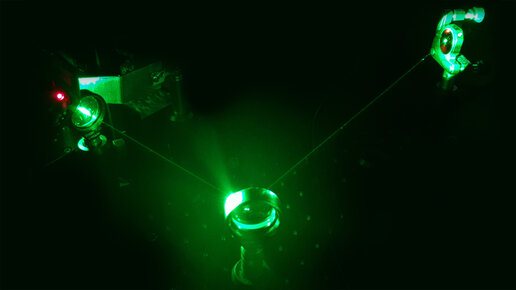
NV-centers are suitable for the observation of such effects that can only be described by quantum physical approaches, even at room temperature. A diamond magnetometer is well suited for a more detailed explanation: NV-centers can assume different charge states in diamond. Starting from a negatively charged NV-center, the electron spin state of the NV center is influenced by an external magnetic field. This is known as the Zeeman effect and also occurs in other materials. In the case of NV-centers, the optical excitation and luminescence light of the optical readout are in the visible light spectrum. Specifically, light of <530 nm will be used for excitation, the fluorescent light has a wavelength of approximately 637 nm. A further improvement in sensitivity can be achieved if an electromagnetic alternating field is coupled in parallel, which further stimulates the emission behavior. The frequency is in the range of 2.9 GHz (microwaves). If the microwave frequency is varied slightly, the magnetic field density can be determined very precisely by evaluating the exact microwave frequency in combination with the luminescence intensity.
Depending on the position of the AFM tip, the intensity of the red luminescence signal can be used to draw conclusions about a specific magnetic property as well as the topology of the material. Research groups from the universities of Saarland, Basel, Stuttgart and Ulm are working on these concepts. The first spin-offs with the approach of marketing such technologies have been founded in Basel and Zurich.
The determination of magnetic fields can be achieved very locally in combination with AFM tips as described above. An alternative design variant consists of a diamond blade with a large numerous of NV-centers, which can be installed in a miniaturized magnetometer. The engineering challenge then consists of optimization and microintegration. First demonstrators show the potential of this approach, which can even be mounted on the tip of an optical waveguide. Other suitable measurement setups can be used to determine further electrical measurement variables directly correlated with the magnetism, e.g. the electrical current & voltage. Since there is also a temperature dependency, e.g. highly localized temperature measurements are possible with the AFM approach.
Recent publications also indicate that further exciting applications can be expected, e.g. in the fields of
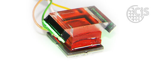
The CiS Research Institute is working in several research projects on the implementation of various demonstrators that use the micro-optical control and readout of NV-centers in diamond, including a matchbox-sized magnetometer for industrial applications (see figures 1 and 2). The CiS Research Institute does not see itself as a manufacturer, but as a partner of industry in the field of applied research and offers its know-how to industrial companies in joint projects. For example, a workshop on applications of quantum technologies took take place in early October 2020.
In the course of these technological possibilities, some of which are on the verge of industrialization, and some of which are new, the question of the availability of the diamond starting material arises. Driven by the jewelry market, two main technologies are currently mainly used for the production of synthetic diamond: chemical vapor deposition (CVD) and the HPHT process, with which diamond stones are synthesized at high pressure and high temperatures. In both cases, these materials require further processing in order to create the NV-centers on the one hand and to obtain the desired geometries on the other. These technologies are available.
The QuApps conference will take place at Düsseldorf Airport from September 13 to 19, 2021. The international event deals with the state of the art and the development of quantum technology. The participants will gain deep insights into current research progress and expected milestones. The conference presents renowned experts in quantum technology, e.g. from IBM Research, Volkswagen Data:Lab, Bosch Research, the University of Stuttgart or Forschungszentrum Jülich. In more than 30 presentations, technologies and applications in the fields of telecommunications, healthcare, security, automotive and others will be discussed. An accompanying exhibition shows possible application examples.
The event is aimed at quantum engineers and researchers, business development strategists and trend scouts in industry, at investors and the interested public. Interested experts are welcome to apply for a presentation or a poster presentation. More information is available at https://quapps-conference.com.
Call for Presentation: Abstracts for oral presentation and posters are accepted. Abstracts must be submitted by email to quapps@ivam.com by May 31, 2021.
